aTDS is composed together with EFEM, Wafer Transfer Robot for full automation in 300mm wafer analysis, and possible to be provided as core component of various options as well as QMS such as 100, 200, 300, 500 amu and so on according to the request of customer.
SILICON WAFERS are the building blocks of modern technology, they provide the substrate onto which circuits are constructed. We offer Prime, Test, Monitor, SEMI standard, and customized silicon wafers in all diameters from 2�¢?�³ to 300mm. Our Wafers meet the SEMI standards, along with customized options.
Silicon On Insulator (SOI) Wafers: Chips fabricated on SOI wafers achieve 30% faster speeds and 80% lower power demands compared to CMOS devices. The SOI structure consists of three layers: a top active device layer for transistor fabrication, a buried oxide (BOX) insulator layer, and a bottom handle wafer layer.
Silicon Float Zone Wafers: is a crystal growth technique that produces highly pure silicon wafers with fewer impurities than traditional methods.
Silicon Thermal Oxide Wafers: Has high quality silicon thermal oxide wafers in all diameters from 2�¢?�³ to 300mm.
Silicon Nitride Wafers: Has different option of film processing for your silicon needs, including LPCVD nitride.
On Insulator (SOI): Has high quality silicon thermal oxide wafers in all diameters from 2�¢?�³ to 300mm.
Fused Silica Wafers: is the amorphous phase of quartz (SiO2).
Borofloat 33 Glass Wafers: is used in a wide range of applications like micro-optics, sensors, microlithography, semiconductor engineering, lighting, medical technology.
GERMANIUM(Ge) WAFERS are semiconductor materials made from Germanium, a group IV element with properties that make it useful in various electronic applications. Historically, Germanium was one of the first materials used in transistors and is still utilized in some specialized applications today, particularly in high-speed electronics and photonics due to its favorable electronic and optical properties.
We offer the following Germanium Wafers:
Undoped Germanium Wafers: Pure Germanium with no intentional doping. These wafers are often used in experimental and research settings to investigate intrinsic semiconductor properties.
N-type Germanium Wafers: Doped with donor impurities (such as phosphorus or arsenic) to increase the concentration of electrons. These wafers are commonly used in transistor applications and other electronic circuits.
P-type Germanium Wafers: Doped with acceptor impurities (such as boron or gallium) to create electronic holes. P-type wafers are often used in diode and transistor applications.
High Purity Germanium Wafers: Extremely low levels of impurities, often used in specialized applications such as radiation detectors and other high-performance devices.
Germanium-on-Insulator (GOI) Wafers: A structure where a thin layer of germanium is bonded to an insulating substrate. This is used to improve device performance and reduce parasitic capacitance.
Thin-Film Germanium Wafers: Thin layers of Germanium material that are used in advanced applications such as flexible electronics and integrated circuits.
A container for carrying semiconductor wafers/silicon wafers, resistant to acid, alkali, and corrosion (strong acid, strong fluoric acid, strong alkali), capable of laser engraving, and able to install RFID. Maintain tracking of carriers and materials.
Mainly used for cleaning, using, and transporting wafers in the acid-base process of semiconductor etching departments.
#wafercleaning #semiconductor #Newenergy #wafers
Made of high-purity resin Teflon, it is resistant to strong acids and alkalis, and can withstand high temperatures: -200~+250C. The surface is smooth, non-stick, and easy to clean. Wafer Container specifications and styles can be customized.
319 Atds (Automated Tds For Semiconductor Wafer) Suppliers
Short on time? Let Atds (Automated Tds For Semiconductor Wafer) sellers contact you.
INDIUM PHOSPHIDE (InP) WAFERS are semiconductor materials made of indium phosphide, a compound semiconductor that is widely used in high-frequency and optoelectronic applications. Due to its efficient electron mobility and direct bandgap properties, InP is favored for devices such as:
High-speed electronics
Laser diodes
Photodetectors
Telecommunications applications, including optical fiber communication
We offer the following InP Wafers:
Undoped InP Wafers: These are pure InP with no intentional doping, used in various applications where intrinsic properties are required.
N-type InP Wafers: Doped with donor impurities (such as tellurium) to increase electron concentration, useful in transistors and high-speed electronics.
P-type InP Wafers: Doped with acceptor impurities (such as zinc) to create holes in the semiconductor, used in light-emitting devices and other optoelectronics.
InP Substrates: Used as a base for growing other semiconductor materials in heterostructures for various applications.
InP Membrane Wafers: Thin layers of InP used for specific applications, including applications in flexible electronics and advanced photonic devices.
InP-based Quantum Dot Wafers: Engineered to create quantum dots that can be used in photonic and optoelectronic devices for enhanced performance.
GaAs Wafers
Gallium Arsenide (GaAs) wafers are critical components in modern electronics and photonics due to their superior electrical and optical properties.
Here�¢??s a focused overview:
GaAs�¢?? is shorthand for Gallium Arsenide, a compound made up of two elements, and the semiconductor used to manufacture GaAs wafers. GaAs is used as a direct bandgap semiconductor, which in layman�¢??s terms, simply means that particles such as electrons can pass through components much quicker and with very little interference. This makes them particularly useful in optical devices because photons, the basic unit for all light, can pass through lenses with ease.
What are GaAs Wafers Use For?
The use of GaAs wafers is dictated by the capabilities of the compound. Because GaAs is a direct bandgap semiconductor, it is especially useful in sensitive electronic equipment that requires amplifying low frequencies. Some of the most common applications for GaAs wafers include:
Sapphire wafers
These are thin slices of synthetic sapphire, commonly used as a substrate in a variety of high-tech applications. Sapphire, which is a crystalline form of aluminum oxide (Al�¢??O�¢??), is valued for its hardness, optical transparency, thermal stability, and chemical resistance. Here�¢??s a brief overview of their applications and properties:
Properties of Sapphire Wafers:
Hardness: Second only to diamond, sapphire is extremely scratch-resistant.
Optical Clarity: Transparent across a wide range of wavelengths (UV to infrared), making it ideal for optical components.
Thermal Stability: Can withstand high temperatures, which is useful in semiconductor processes.
Chemical Resistance: Highly resistant to acids and alkalis, ensuring durability in harsh environments.
Electrical Insulation: Sapphire is an excellent electrical insulator.
Talc is an amazingly variable mineral with a massive range of uses across several industries. It is the softest rock on the planet. Softness, water repellency, chemical inertness, platyness, and an affinity for organic compounds are all characteristics of talc
Talc is a highly desired multi-functional filler and process facilitator in a wide range of applications, including plastics, paper, ceramics, and paint.
The physical properties of talc are softness as it ranks 1 on the Mohs scale, natural affinity with oils making it an excellent hydrophobic mineral and its chemical inertness.
It is an extremely useful mineral in the manufacturing of solar panels, semiconductors and electronics, aluminium and steel alloys, and also in the construction sector, after being transformed into silicon (Si) through gaseous reduction at high temperatures.
Aryan Tiles is one of the biggest producers and suppliers for talc in India. We extract our talc mineral from several regions of Rajasthan. Our scientists and process experts collaborate with customers to develop innovative minerals that satisfy their specific industriesâ?? needs.
Talc, or talcum, is a clay mineral, composed of hydrated magnesium silicate with the chemical formula Mgâ??Siâ??Oâ??â??(OH)â??
Talc provide the ideal blend of stiffness and impact strength, allowing producers to create parts that are both thinner and lighter and thus reducing overall vehicle weight within the automation sector. It also improves rubber permeability, lowers tyre rolling resistance and increases vehicle fuel efficiency.
Further in the paints and coatings, talc works as an excellent natural alternative to less environmentally friendly TiO2 for increasing coating mechanical and optical qualities.
Moreover, in the pulp and paper industry, talc is great for preventing deposits, allowing mills to operate in closed water circuits, and maximizing prime resources.
Furthermore, in the ceramic tiles and sanitary ware, talc improves vitrification, allowing manufacturers to lower firing temperatures and shorten firing cycles.
In the agriculture industry, talc-based mineral solution works as natural alternatives to pesticides for preserving fruit from the sun's rays and diseases. They are perfect for organic agriculture. Talcs are also used to make fertilizer flow and anti-caking agents.
Talc has wide range of applications within several industries. And, our production and supply of talc mineral are innovative and of premium quality. We have been able to cater to the specified needs with our years of technical expertise.
Seawater desalination solution
Brackish Water Reverse Osmosis Solution
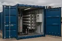
BW is a modular, containerized Brackish Water Reverse Osmosis (BWRO) system, designed for efficient and flexible water desalination in various sectors.
BWRO is a type of desalination process that utilizes reverse osmosis membranes to remove dissolved salts and other impurities from brackish water.
Key Features
Modular & Scalable: Housed in 40-foot containers, easy to transport, install, and expand.
Flexible Feedwater Tolerance: Handles water with up to 10,000 ppm TDS, including well and surface water.
High Efficiency:
Recovery rate: Up to 90%
Energy use: As low as 0.65 kWh/m
Two Main Models:
BW LS (Low Salinity): Up to 3,700 ppm TDS
BW HS (High Salinity): Up to 10,000 ppm TDS
Capacities Available: 1,000 or 20,000 m/day
Availability: 97%
Automation: Fully automated with PLC/HMI and remote monitoring
The system is a modular, containerized seawater desalination system designed for rapid deployment, low environmental impact, and high efficiency. Housed in standard 40-foot ISO containers, these units provide pre-treatment, reverse osmosis (RO), and energy recovery in a compact form, ideal for industrial, municipal, commercial, and remote sites.
________________________________________
Key Features & Advantages:
Cost-effective: Pre-assembled units minimize setup time and costs.
Sustainable: Low energy and chemical consumption with up to 50% recovery rate.
Compact & Scalable: Small footprint enables flexible deployment and easy expansion.
Smart Operations: Fully automated with remote monitoring, alerts, and centralized control options.
System Options:
Pretreatment: DAF, multimedia filters, activated carbon, clarification
Post-treatment: Remineralization, pH adjustment, UV/chlorine disinfection
________________________________________
Deployment Models:
The unit, scalable up to 20,000 m/day.
Applications
Ideal for:
Municipalities
Resorts, hotels, golf clubs
Construction sites
Industrial plants
Agriculture & irrigation
Mining & oil/gas operations
________________________________________
System Options
Pre-treatment: Hypochlorite dosing, solids/oil removal
Post-treatment: Remineralization, pH adjustment, chlorination
Monitoring & Control: Remote access, real-time alerts, data reporting
________________________________________
Advantages
Low capital (CAPEX) and operational (OPEX) costs
Fast deployment and commissioning
Low environmental impact
Easily scalable for large-scale or decentralized solutions
________________________________________
Note: The prices provided are for reference only and may be subject to change.
Acetonitrile is an organic compound with the molecular formula CH3CN or c2h3n. It is a colorless liquid, highly volatile, with a special smell similar to ether, excellent solvent performance, and can dissolve a variety of organic, inorganic and gaseous substances. It has certain toxicity and is infinitely miscible with water and alcohol. Acetonitrile is an important organic intermediate, which can undergo typical nitrile reactions and is used to prepare many typical nitrogen-containing compounds. Acetonitrile can be used as a solvent for the synthesis of vitamin A, cortisone, carboamine drugs and their intermediates, and also as an active medium solvent for the manufacture of vitamin B1 and amino acids. It can replace chlorinated solvent. It is used in vinyl coating, fatty acid extractant, alcohol denaturant, butadiene extractant and solvent of acrylonitrile synthetic fiber. It is also used in fabric dyeing, lighting, perfume manufacturing and photosensitive material manufacturing.
Chemical analysis and instrumental analysis
Acetonitrile is an organic modifier and solvent used in thin layer chromatography, paper chromatography, spectroscopy and polarographic analysis in recent years. Since high-purity acetonitrile does not absorb ultraviolet light at 200nm ~ 400nm, an application being developed is as a solvent for high-performance liquid chromatography HPLC, which can make the analytical sensitivity as high as 10-9 levels.
Intermediate of synthetic medicine and pesticide
Acetonitrile can be used as an intermediate in the synthesis of various medicines and pesticides. In medicine, it is used to synthesize a series of important pharmaceutical intermediates, such as vitamin B1, metronidazole, ethambutol, aminopteridine, adenine and antitussive; In pesticides, it is used to synthesize pyrethroid insecticides, acetaminophen and other pesticide intermediates.
Semiconductor cleaning agent
Acetonitrile is an organic solvent with strong polarity. It has good solubility in grease, inorganic salt, organic matter and polymer compounds. It can clean grease, wax, fingerprints, corrosive agent and flux residues on silicon wafers. Therefore, high purity acetonitrile can be used as semiconductor cleaner.
It is easy to use for the automation of analyzing processes.
The overall efficiency of analysis increases with shortened time for analysis.
The buffer zone keeps the process zone vacuum all the time, so the inflow of dirty gas from outside is minimized and the precision of analysis becomes maximized.
Keeping the process zone vacuum delays the aging of heater components more than before, so it is good for cost reduction.
The automation of analysis processes maximizes the utility of time of testing manpower.
Minimizing the contact of samples for analysis to the outside minimizes contamination.
The increase of analysis efficiency actualizes the dedtion of faultiness in advance, so it is possible to test the processes.
High Purity Quartz Sand, meticulously produced from premium natural quartz using advanced purification technology, ensuring a purity 98% to 99.9%. Its unique crystal structure and lattice pattern impart remarkable characteristics such as high-temperature resistance, low coefficient of thermal expansion, excellent insulation, and corrosion resistance. High Purity Quartz Sand finds extensive application as a crucial raw material in integrated circuits, semiconductor chips, photovoltaic fibers, innovative glass production, and various fields.
High Purity Quartz Sand Applications
1) Semiconducto r Industry â?? manufacture of substrates for transistors, integrated circuits, micro electric, and semiconducto r devices
2) Optical glass â?? manufacture of high-quality optical devices such as optical lenses, optical windows, laser devices
3) Solar Energy Industry â?? manufacturing of solar cells, base material for silicon wafers
4) Ceramic Materials â?? manufacturing of ceramic tiles, high strength high wear resistant ceramic products, porcelain
5) Chemical Industry â?? used in catalytic process and chemical reactions.
6) Electronics Industry â?? manufacture of electronic devices
Hydrofluoric Acid 49% Solution is a colorless liquid. Hydrofluoric Acid, 49% Solution, contains 49% Hydrofluoric Acid mixed with a balanced quantity of Water. It can be used for the electronic industry to perform cleaning of silicon wafers and etching of semiconductors, as these delicate applications require ultra-purified solvents. Hydrofluoric acid is used in a variety of over-the-counter products such as toilet bowl cleaners, concrete cleaners, and metal polishes. However, the uses for industrial applications are far more numerous. hydrofluoric acid is used for quartz purification, glass etching, refrigerant manufacturing, pharmaceuticals, high octane gasoline, aluminum production, plastics, electrical components, and fluorescent light bulbs.
Specifications
Appearance: Clear liquid.
Hydrofluoric Acid: 49% Min
Fluorosilicic Acid (H2SiF6): 0.5% Max
Sulfur Dioxide: 0.007% Max
Sulfuric Acid (H2SO4): 0.08% Max
Packing
500/507.508 lb drum, 4 drums per pallet
DOT Transportation
Acetonitrile is an organic compound with the molecular formula CH3CN or c2h3n. It is a colorless liquid, highly volatile, with a special smell similar to ether, excellent solvent performance, and can dissolve a variety of organic, inorganic and gaseous substances. It has certain toxicity and is infinitely miscible with water and alcohol. Acetonitrile is an important organic intermediate, which can undergo typical nitrile reactions and is used to prepare many typical nitrogen-containing compounds. Acetonitrile can be used as a solvent for the synthesis of vitamin A, cortisone, carboamine drugs and their intermediates, and also as an active medium solvent for the manufacture of vitamin B1 and amino acids. It can replace chlorinated solvent. It is used in vinyl coating, fatty acid extractant, alcohol denaturant, butadiene extractant and solvent of acrylonitrile synthetic fiber. It is also used in fabric dyeing, lighting, perfume manufacturing and photosensitive material manufacturing.
Chemical analysis and instrumental analysis
Acetonitrile is an organic modifier and solvent used in thin layer chromatography, paper chromatography, spectroscopy and polarographic analysis in recent years. Since high-purity acetonitrile does not absorb ultraviolet light at 200nm ~ 400nm, an application being developed is as a solvent for high-performance liquid chromatography HPLC, which can make the analytical sensitivity as high as 10-9 levels.
Intermediate of synthetic medicine and pesticide
Acetonitrile can be used as an intermediate in the synthesis of various medicines and pesticides. In medicine, it is used to synthesize a series of important pharmaceutical intermediates, such as vitamin B1, metronidazole, ethambutol, aminopteridine, adenine and antitussive; In pesticides, it is used to synthesize pyrethroid insecticides, acetaminophen and other pesticide intermediates.
Semiconductor cleaning agent
Acetonitrile is an organic solvent with strong polarity. It has good solubility in grease, inorganic salt, organic matter and polymer compounds. It can clean grease, wax, fingerprints, corrosive agent and flux residues on silicon wafers. Therefore, high purity acetonitrile can be used as semiconductor cleaner.
semiconductor si wafers
prime grade/high quality
diameter from 2" to 12"
ultra thin or ultra thick
crystalline orientation <100>, <111>, <110>
most resistivity range