Dear Friends,
Our company specializes in producing High Mix & Medium-small series Rigid PCBs(1-28layers),Rigid-flex pcbs as well as AL pcbs in China .
As a Sales Manager in my company, I have worked in PCB industry over than 10year since my graduation from University .
We exported a lot of PCBs to Europe and America countries for several years .
I expect to know more parnters all over the world through here.
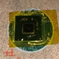
We just processed in a large batch of chipsets. I posted below current inventory and attached pictures of each type of chipset. Please review and let me know your interest/offer.
Chipset 1 (H61) â?? 3,350 units
Chipset 2 (H81) â?? 2,206 units
Chipset 3 (H55) â?? 436 units
Chipset 4 (B250) â?? 1,600 units
Chipset 5 (SR406) â?? 345 units
All weather traction
Enhanced controllability
Fuel efficient drive
Excellent durability
The Hankook Smart Flex AH35 is a highway terrain all-season tire manufactured for commercial vehicles. The tyre model is made to be mounted on the vehicle's steering axle.
Hankook Smart Flex AH35 - Key Features
All-Weather Performance: The tire offers reliable traction in dry, wet, and winter conditions, thanks to its wide grooves and 3D sipes, which also prevent hydroplaning.
Enhanced Control: The ribbed tread design ensures constant road contact, improving steering response and driving stability.
Fuel Efficiency: The optimized 3D siping reduces rolling resistance, leading to lower fuel consumption and CO2 emissions.
Durability: Reinforced carcass structure maintains the tire's shape under heavy loads, extending tread life and making it cost-efficient.
As a PCB Supplier for more than 8 years, Fulltronics are very professional, not only in PCB production, but also in after-sales service and logistic, our advantages show as following:
1. Quotation for multilayer PCB within 12 hours, urgent offer within 1 hours;
2. Rich experiences in multilayer PCB, professional suggestions from design stage in order to avoid any impracticable design;
3. Rich experience as PCB supplier enhances our understanding of oversea clients' requests;
4. Only use of superior quality materials in our factory;
5. Different from other PCB suppliers, we can accept sample order, small series, as well as mass production;
6. Experienced engineering team clear EQ/TQ at quick time;
7. Individual QCs at factories to follow production and double check semi-finished & finished PCBs to ensure good quality;
8. Logistic department will ensure your PCBs to be delivered in earliest time and lowest shipping cost.
Place of origin:Guangdong china (mainland)Brand name:FastpcbaModel number:Pcb
Base material:Alu, fr4, cem3
Copper thickness:0.3-3oz
Board thickness:0.3-6mm
Min. Hole size:0.2mm
Min. Line width:3mil
Min. Line spacing:3mil
Surface finishing:
Hasl, osp, immersion gold/au, immersion silver, etc.
Product name:Pcb
Pcb:Customized
Pcb tolerance of finished thickness:¡À5%Hole tolerance: pth:¡À0.075, ntph:¡À0.05
Solder mask:Green/black/white/red/blue/yellow
Max board size:1200mm*600mm
Profiling punching:Routing, v-cut, beveling
Layer count:1-22
Wrap and twist:5%
Pcb standard:Ipc-a-610 e class ii-iii
Pcba board packed with inner vacuum packing, outer standard carton box , special packages requested.
What is HDI PCB
High density interconnect (HDI) PCB, represent one of the fastest growing technologies in PCBs. Because of its higher circuitry density than traditional circuit boards, the HDI PCB design is able to incorporate smaller vias and capture pads, and higher connection pad densities. HDI Boards contain blind and buried vias and often contain micro vias of 0.006 or less in diameter.
By using HDI technology, designers now have the ability to place more components on both sides of the raw PCB if desired. Now as the development of via in pad and blind via technology, it allow designers to place smaller components closer together. This means faster transmission of signals and a significant reduction in signal loss and crossing delays.
HDI PCB is regularly found in mobile phones, touch-screen devices, laptop computers, digital cameras, 4G network communications, also prominently featured in medical devices.
Advantages of HDI PCB
The most common reason for using HDI technology is a significant increase in packaging density. The space that obtained by finer track structures is available for components. In addition, overall space requirements are reduced will result in smaller board sizes and fewer layers.
Usually FPGA or BGA are available with 1mm or less spacing. HDI technology makes routing and connection easy, especially when routing between pins.
Service at tendtronic dot c0m
Tendtronic corporation ltd. A leading pcb manufacturer located in shenzhen china. We focus in pcb industry over 10 years(established in 2003, shenhuaguo), base on iso9001 management system, stable quality, good after-sale service, we had gain very good reputation from our cooperated partners, such as hai’er, tcl, miui mobile oem factory, fsl lighting……
We trust that our service will help you to win more market shares too.Your factory visit before production will be highly welcome!
Now we are ready to offer free sample or sample free shipping or even both services for you.(needs assessment
Just take a minute to send your pcb quick quotations (attachment) and gerber file to:
Jun(at)tendtronic(dot)com
We have full confidence that you will choose us after getting our quality sample.
Waiting for your soon reply and kindly comment here.
Tendtronic corporation ltd. A leading pcb manufacturer located in shenzhen china. We focus in pcb industry over 10 years(established in 2003, shenhuaguo), base on iso9001 management system, stable quality, good after-sale service, we had gain very good reputation from our cooperated partners, such as hai’er, tcl, miui mobile oem factory, fsl lighting……
We trust that our service will help you to win more market shares too.Your factory visit before production will be highly welcome!
Now we are ready to offer free sample or sample free shipping or even both services for you.needs assessment
Just take a minute to send your pcb quick quotations (attachment) and gerber file to:
Jun(at)tendtronic(dot)com
We have full confidence that you will choose us after getting our quality sample.
Waiting for your soon reply and kindly comment here.
Ezpcb capability:
Layers:1-40
Materials:fr-4, fr-1, cem-1, cem-3, teflon, rogers, al base
Max. Board size:550mm x 710mm
Board thickness:0.15mm-5mm
Finished copper thickness:1/2oz-10oz
The min. Track:3mil (0.075mm)
The min. Clearance:3mil (0.075mm)
The min. Hole diameter:0.10mm
Finish:hasl, gold plated, immersion gold/silver
Blind/Buried Via
5+N(N+M)+5 Structure
Trace Width/Spacing 1.6/1.6mil
Laser Hole Size(mm) 0.075
High Density Interconnector
Founded in 2007, PEAK Co.,Ltd is an electronic solutions company offering 1-64 layers PCB fabrication, assembly, testing & validation of rigid, rigid-flex, HDI, high frequency, high speed, metal core, IC substrate, substrate-like and other special PCB. Our modern 54,000 square foot manufacturing facility allows us to provide all rigid & rigid-flex services under one roof and offer quick-turn capabilities.PEAK has a professional reputation for developing high-performance solutions for technically advanced OEM's in a variety of markets including aerospace and defense, medical, computer, communication, server, semiconductor IC, automotives, industrial control, optoelectronics, LED and others.
8 layer 1mm HDI PCB 0 gap
8 layer PCB, 0 gap PCB, 1mm PCB
1) Thickness: 0.1mm-5mm
2) Minimum linewidthï¼?0.075mm/3mil
3) Minimum gapï¼?0.065/2.8mil
4) Minimum aperture inradiumï¼?0.15mm
5) Minimum aperture external diameterï¼?0.45mm
6) Minimum BGA: 0.2mm
7) Layerï¼?4 layers through hole non-impedance
All multilayer boards are printed with 36t screen, the resistance welding oil is 50 tons thicker than the traditional 43t, which provides reliability guarantee for the bga and more precise fine lines.