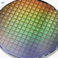
INDIUM PHOSPHIDE (InP) WAFERS are semiconductor materials made of indium phosphide, a compound semiconductor that is widely used in high-frequency and optoelectronic applications. Due to its efficient electron mobility and direct bandgap properties, InP is favored for devices such as:
High-speed electronics
Laser diodes
Photodetectors
Telecommunications applications, including optical fiber communication
We offer the following InP Wafers:
Undoped InP Wafers: These are pure InP with no intentional doping, used in various applications where intrinsic properties are required.
N-type InP Wafers: Doped with donor impurities (such as tellurium) to increase electron concentration, useful in transistors and high-speed electronics.
P-type InP Wafers: Doped with acceptor impurities (such as zinc) to create holes in the semiconductor, used in light-emitting devices and other optoelectronics.
InP Substrates: Used as a base for growing other semiconductor materials in heterostructures for various applications.
InP Membrane Wafers: Thin layers of InP used for specific applications, including applications in flexible electronics and advanced photonic devices.
InP-based Quantum Dot Wafers: Engineered to create quantum dots that can be used in photonic and optoelectronic devices for enhanced performance.
GaAs Wafers
Gallium Arsenide (GaAs) wafers are critical components in modern electronics and photonics due to their superior electrical and optical properties.
Here�¢??s a focused overview:
GaAs�¢?? is shorthand for Gallium Arsenide, a compound made up of two elements, and the semiconductor used to manufacture GaAs wafers. GaAs is used as a direct bandgap semiconductor, which in layman�¢??s terms, simply means that particles such as electrons can pass through components much quicker and with very little interference. This makes them particularly useful in optical devices because photons, the basic unit for all light, can pass through lenses with ease.
What are GaAs Wafers Use For?
The use of GaAs wafers is dictated by the capabilities of the compound. Because GaAs is a direct bandgap semiconductor, it is especially useful in sensitive electronic equipment that requires amplifying low frequencies. Some of the most common applications for GaAs wafers include:
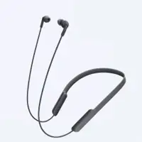
In-ear headphones with wireless Bluetooth connectivity
Bring exhilarating music experiences into your daily life. EXTRA BASS sound makes every track exciting, while the wireless connectivity and lightweight design help you listen comfortably anywhere
With its twin 1.18 in drivers and bass booster, these headphones deliver big sound without breaking a sweat. Plus the in-line remote with mic lets you take control of your smartphones music and calls.
Driver unit
1.18 in (dome type)
Frequency response (hz)
522,000 hz
Cord length
Approx. 3.94 ft
We have over 800 tested working desktop computers in stock. Please send me an email, and I will reply with the complete line item list for you to bid on.
6327 Computer Chairs Suppliers
Short on time? Let Computer Chairs sellers contact you.
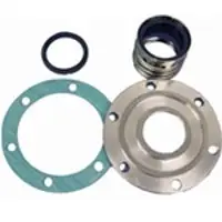
Shaft seal assembly for carrier 5H40 through 5H86 Models
Replacement shaft seal assembly for carrier 5H Models, OEM Ref: 5H40-276, Fits 5H40,46,60,66,80,86,
Includes seal, seal plate and klinger gasket
CMP: SEL-0645 / Bradleys 9405