We have over 800 tested working desktop computers in stock. Please send me an email, and I will reply with the complete line item list for you to bid on.
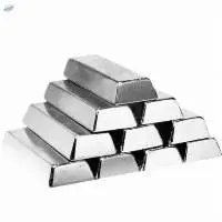
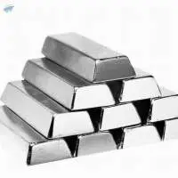
High-Purity A8 Aluminum Ingots (99.80% min. Al Content)
Brand Name: RIO TINTO ALUMINUM
Origin: Australia
________________________________________
Chemical Composition:
Al 99.80% (minimum)
Silicon (Si) 0.05%
Iron (Fe) 0.20%
Copper (Cu) 0.01%
Manganese (Mn) 0.01%
Magnesium (Mg) 0.03%
Zinc (Zn) 0.03%
Titanium (Ti) 0.03%
Others (each) 0.03%
Others (total) 0.10%
________________________________________
Product Form & Packaging
Form: Standard trapezoidal aluminum ingots
Unit Weight: Approx. 22.5 â?? 23.5 kg per ingot
Bundle: 1,000 kg strapped bundles on wooden pallets
Custom Branding: Optional with MOQ
________________________________________
Logistics & Delivery
Packaging: Export-grade seaworthy packaging
Incoterms: CIF
Lead Time: 15â??25 days from order confirmation (subject to availability)
________________________________________
A8 aluminum ingots are ideal for:
Wire and cable production
Conductors and electrical applications
Re-rolling for sheets, foils, and extrusions
High-performance casting applications
________________________________________
Certifications
ISO 9001:2015
LME-aligned product quality
6205 Computer Cables Suppliers
Short on time? Let Computer Cables sellers contact you.
Product Specifications:
Grade A7
Purity (Al Content) 99.7% (minimum)
Form Rectangular ingots with lifting notches or grooves
Weight per Ingot 15-25 kg (or as per buyer request)
Bundle Weight ~1000 kg strapped with steel bands
Color Silvery-white, smooth surface, free of cracks or inclusions
Surface Condition Clean, dry, free from oil, oxidation, or contamination
Melting Point ~660.3 C
Appearance Bright metallic luster, no visible slag or shrinkage
Chemical Composition (in % by weight):
Aluminum (Al) 99.70%
Silicon (Si) 0.10%
Iron (Fe) 0.20%
Copper (Cu) 0.01%
Zinc (Zn) 0.02%
Manganese (Mn) 0.01%
Magnesium (Mg) 0.01%
Titanium (Ti) 0.03%
Other (each) 0.03%
Total Others 0.30%
Containerization: Suitable for 20ft or 40ft containers
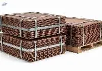
High-purity Electrolytic Copper Cathodes (Grade A, 99.99%) sourced directly through primary electro-refining producers. Material is suited for electrical wire rod manufacturing, cable processing, and specialized metallurgical alloys. Every shipment is backed by mandatory third-party origin and discharge port inspection (SGS / Intertek / CCIC) covering chemical purity, bundle counts, and weight.
PRICING MECHANISM: London Metal Exchange (LME) Cash Settlement Price minus tiered volume discount (up to LME - 7% for orders of 2,000 MT/month and above). Final contract pricing calculated on the official cash settlement average 3 banking days prior to Bill of Lading (B/L) date.
PAYMENT TERMS: 100% Irrevocable, Transferable or Non-Transferable Sight Letter of Credit (MT700 DLC) issued by Tier-1 Prime Bank; final settlement via Telegraphic Transfer (MT103 TT) post-SGS destination port assay.
PERFORMANCE BOND: 2% Performance Guarantee (PBG) issued by Seller's bank upon receipt of operative LC.
LSRC2004 Aerospace MIL-1394b High-Rate Data Cable
Cable applications: flight control, mission systems, data bus, avionics network, propulsion control
Category:MIL-STD-1394b high-speed bus series
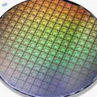
INDIUM PHOSPHIDE (InP) WAFERS are semiconductor materials made of indium phosphide, a compound semiconductor that is widely used in high-frequency and optoelectronic applications. Due to its efficient electron mobility and direct bandgap properties, InP is favored for devices such as:
High-speed electronics
Laser diodes
Photodetectors
Telecommunications applications, including optical fiber communication
We offer the following InP Wafers:
Undoped InP Wafers: These are pure InP with no intentional doping, used in various applications where intrinsic properties are required.
N-type InP Wafers: Doped with donor impurities (such as tellurium) to increase electron concentration, useful in transistors and high-speed electronics.
P-type InP Wafers: Doped with acceptor impurities (such as zinc) to create holes in the semiconductor, used in light-emitting devices and other optoelectronics.
InP Substrates: Used as a base for growing other semiconductor materials in heterostructures for various applications.
InP Membrane Wafers: Thin layers of InP used for specific applications, including applications in flexible electronics and advanced photonic devices.
InP-based Quantum Dot Wafers: Engineered to create quantum dots that can be used in photonic and optoelectronic devices for enhanced performance.
GaAs Wafers
Gallium Arsenide (GaAs) wafers are critical components in modern electronics and photonics due to their superior electrical and optical properties.
Here�¢??s a focused overview:
GaAs�¢?? is shorthand for Gallium Arsenide, a compound made up of two elements, and the semiconductor used to manufacture GaAs wafers. GaAs is used as a direct bandgap semiconductor, which in layman�¢??s terms, simply means that particles such as electrons can pass through components much quicker and with very little interference. This makes them particularly useful in optical devices because photons, the basic unit for all light, can pass through lenses with ease.
What are GaAs Wafers Use For?
The use of GaAs wafers is dictated by the capabilities of the compound. Because GaAs is a direct bandgap semiconductor, it is especially useful in sensitive electronic equipment that requires amplifying low frequencies. Some of the most common applications for GaAs wafers include:
In-ear headphones with wireless Bluetooth connectivity
Bring exhilarating music experiences into your daily life. EXTRA BASS sound makes every track exciting, while the wireless connectivity and lightweight design help you listen comfortably anywhere
With its twin 1.18 in drivers and bass booster, these headphones deliver big sound without breaking a sweat. Plus the in-line remote with mic lets you take control of your smartphones music and calls.
Driver unit
1.18 in (dome type)
Frequency response (hz)
522,000 hz
Cord length
Approx. 3.94 ft